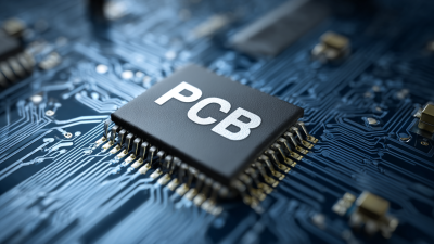
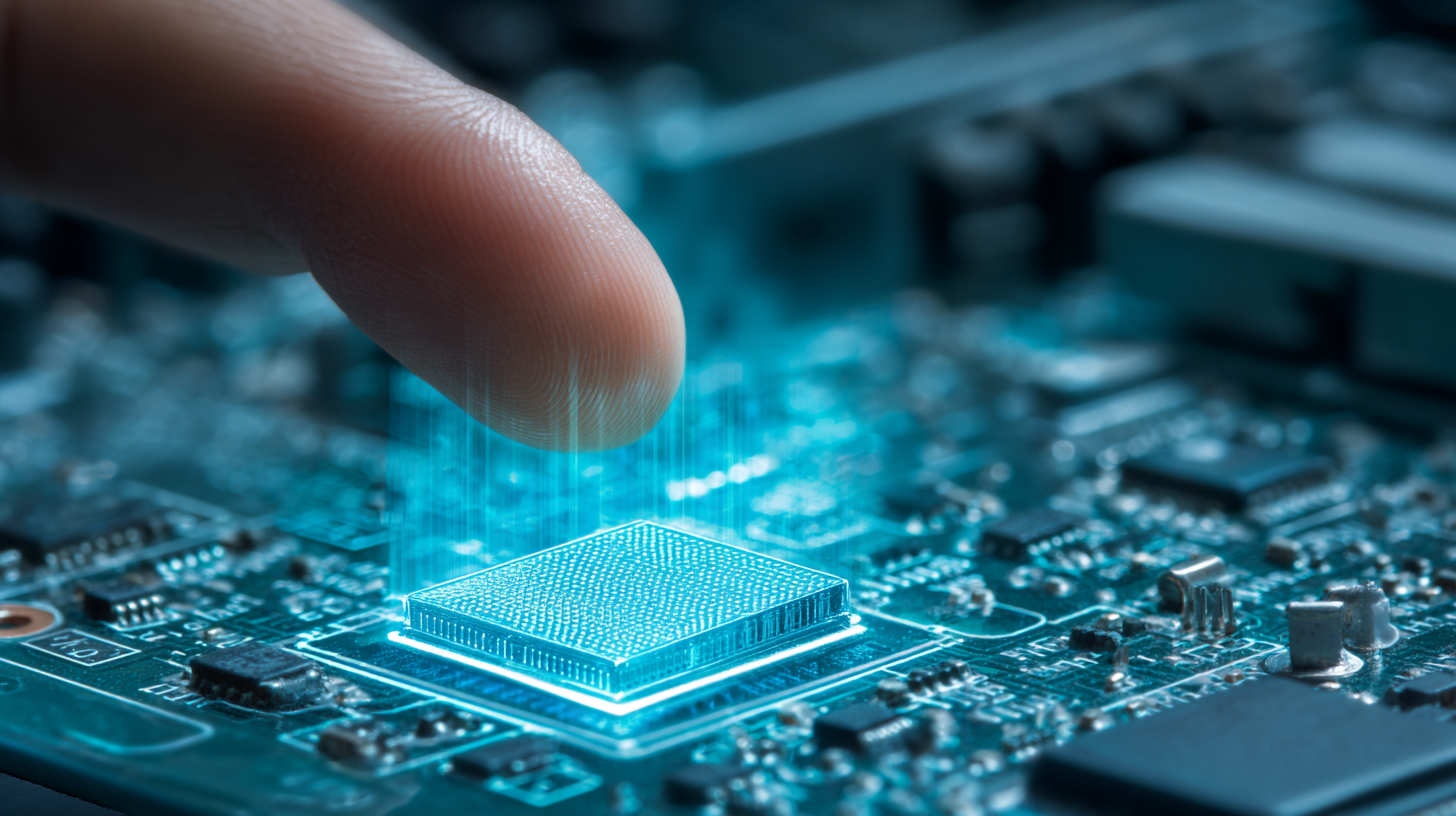
Exploring the Future of Pcb Touch Buttons: Innovative Applications and Technology Advances
The advancements in PCB touch buttons are transforming the landscape of human-machine interaction, prompting a notable surge in their applications across various sectors. According to a recent market report by Research and Markets, the global touch button market is anticipated to grow from $2.5 billion in 2021 to $4.8 billion by 2026, reflecting a compound annual growth rate (CAGR) of 14.5%. This growth is driven by the increasing demand for user-friendly interfaces in consumer electronics, automotive dashboards, and home automation systems. As manufacturers strive for innovative solutions, PCB touch buttons are being engineered with enhanced sensitivity, durability, and aesthetic appeal. Emerging technologies, such as haptic feedback and capacitive sensing, are contributing to these developments, leading to more precise interactions and a richer user experience. This paper delves into the future of PCB touch buttons, exploring innovative applications and the technological advancements that are set to redefine their role in various industries.
The Rise of Touch Button Technology in Consumer Electronics: A Market Overview
 The rise of touch button technology in consumer electronics has revolutionized user interfaces across various devices. According to a global market report by MarketsandMarkets, the touch button market is projected to grow from USD 2.1 billion in 2021 to USD 3.7 billion by 2026, reflecting a compound annual growth rate (CAGR) of 11.6%. This significant growth can be attributed to the increasing demand for user-friendly interfaces and the proliferation of smart devices, where intuitive interaction is essential. Industry leaders such as Apple and Samsung have adopted capacitive touch buttons, enhancing user experience by integrating seamless touch functionality into smartphones and wearables.
Tips: When designing touch buttons for consumer electronics, consider the ergonomics of button placement. Ensuring that buttons are easily accessible can enhance usability and overall customer satisfaction. Additionally, incorporating
haptic feedback can create a more immersive experience, mimicking the tactile sensation of traditional buttons.
Innovative applications of touch button technology are also emerging in home automation. Smart home devices are increasingly utilizing touch controls, allowing users to manage lighting, security, and climate with ease. Furthermore, a report from ResearchAndMarkets predicts that the smart home market will reach USD 174 billion by 2025, with touch technology playing a vital role in this growth. By integrating advanced touch technology, manufacturers can meet consumer expectations for convenience and connectivity while supporting a seamless smart ecosystem.
Tips: For manufacturers entering the smart home market, prioritizing compatibility with existing ecosystems such as Google Home and Amazon Alexa can drive adoption and attract a broader consumer base.
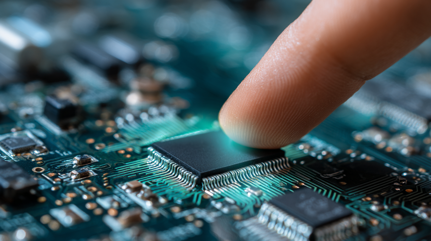
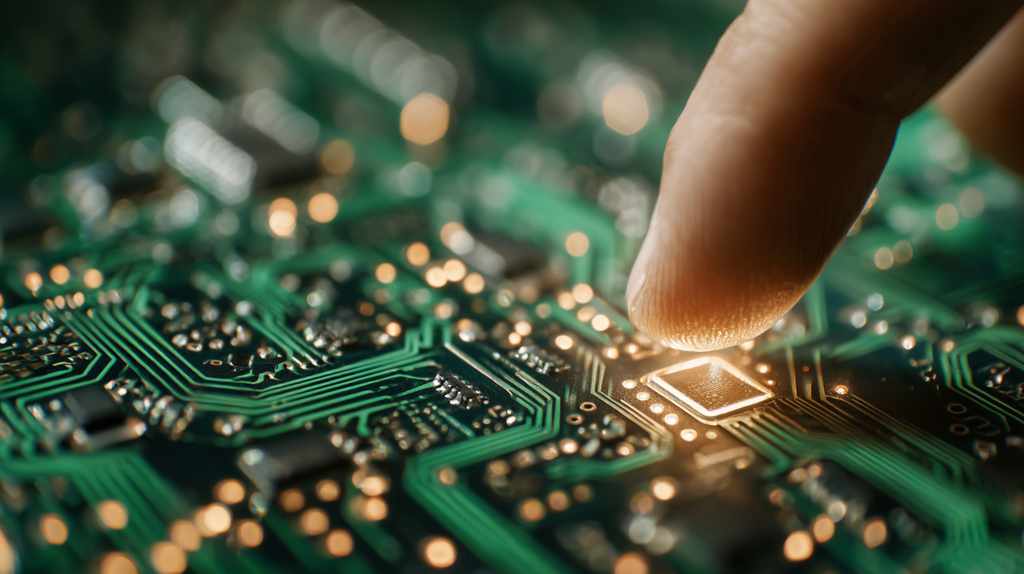
Advancements in PCB Design: Enhancing Touch Sensor Sensitivity and Durability
The evolution of printed circuit board (PCB) technology has significantly improved the sensitivity and durability of touch sensors, making them more reliable and adaptable for various applications. According to a report by MarketsandMarkets, the global market for touch sensors is expected to grow from $12.6 billion in 2020 to $19.6 billion by 2025, driven by advances in PCB design and materials. Enhanced sensitivity allows for more responsive interfaces, improving user experience in devices like smartphones and smart home appliances.
In addition to sensitivity, durability is a critical factor in PCB design, especially for devices subjected to frequent use. Recent innovations, such as the integration of flexible substrates and protective coatings, have led to touch sensors that withstand harsher environments without compromising performance. A study from ResearchAndMarkets indicates that the use of advanced materials like polyimide in PCB manufacturing can increase lifespan significantly, often exceeding five million actuations.
**Tip:** When designing PCBs for touch applications, consider using a combination of rigid and flexible materials to enhance both sensitivity and durability without adding excessive weight.
**Tip:** Choose protective coatings that are not only scratch-resistant but also anti-fingerprint, maintaining user interfaces that remain clean and functional over time.
Exploring the Future of PCB Touch Buttons: Innovative Applications and Technology Advances
| Application |
Sensitivity Level |
Durability Rating |
Current Technology Used |
Future Trends |
| Consumer Electronics |
High |
5 Years |
Capacitive Touch Sensing |
Gesture Recognition |
| Smart Home Devices |
Medium |
3 Years |
Resistive Touch Sensing |
Integration with AI |
| Automotive Controls |
High |
7 Years |
Projected Capacitive Technology |
Touchless Operation |
| Industrial Equipment |
Medium |
10 Years |
Infrared Touch Sensing |
Increased Resilience |
| Healthcare Devices |
Very High |
5 Years |
Multi-Touch Capabilities |
Bio-Feedback Integration |
Innovative Applications of Touch Buttons in Smart Home Devices and IoT
The rise of smart home devices and the Internet of Things (IoT) is revolutionizing how we interact with our living environments, making touch buttons an essential feature in this transition. As the global gesture recognition market is projected to grow from $31.05 billion in 2025 to an impressive $182.47 billion by 2032, the demand for intuitive control systems is becoming increasingly critical. Touch buttons, as user interfaces, are at the forefront of this evolution, facilitating seamless integration with other smart home technologies.
Innovative applications of touch buttons extend beyond mere convenience. They enhance user experience by providing tactile feedback and intuitive control over multiple smart devices within the home. Latest advancements emphasize not only functionality but also aesthetics, allowing for customizable designs that suit various home decors. The emerging control interfaces from major tech companies aim to transform the way users manage their smart homes, moving from complex mobile apps to straightforward in-home solutions, ultimately making technology more accessible for everyone. As the industry evolves, the implication of these advancements is significant—they promise to simplify our interactions with technology while increasing the functionality of smart homes.
Future Trends: Biometric Integration and Haptic Feedback in Touch Interfaces
The future of PCB touch buttons is poised for remarkable advancements, particularly through the integration of biometric technologies and haptic feedback systems. Reports project that the adoption of biometric authentication in electronic devices will grow at a CAGR of around 20% by 2025, driven by increasing demand for user security and seamless interaction. This trend is set to redefine how users engage with their devices, as touch interfaces evolve to include features like fingerprint recognition and facial identification directly within touch buttons.
Haptic feedback technology will further enhance user experience by simulating tactile sensations, making touch interactions more intuitive and satisfying. According to recent market analyses, the haptic technology sector is expected to reach approximately $12 billion by 2024, attributed to its incorporation in smartphones, wearables, and automotive interfaces. Integrating haptic feedback with PCB touch buttons not only enriches user interaction but also provides vital feedback, improving accessibility for visually impaired users.
**Tips:** To stay ahead in this evolving landscape, consider exploring partnerships with tech innovators focused on biometric and haptic solutions. Additionally, investing in user-centered design approaches will ensure your products meet the expectations of a tech-savvy audience while enhancing usability and security.
Future Trends in PCB Touch Buttons: Biometric Integration and Haptic Feedback
Sustainability in PCB Production: Eco-Friendly Materials and Manufacturing Techniques
The growing demand for sustainable practices in the electronics industry has prompted a significant shift towards eco-friendly materials and manufacturing techniques for Printed Circuit Boards (PCBs). By utilizing biodegradable substrates and recyclable materials, manufacturers can reduce the environmental impact associated with traditional PCB production. Innovations in material science, such as bio-based resins and lead-free solder, are leading the way in creating durable yet sustainable components that meet the performance standards of modern technology.
In addition to material innovations, the manufacturing process itself is being overhauled to enhance sustainability. Techniques such as automated assembly and additive manufacturing reduce waste and energy consumption, while the implementation of closed-loop systems allows for the recycling of PCB scraps and minimizing hazardous waste. Furthermore, advancements in digital design tools enable the optimization of PCB layouts for minimal material usage without sacrificing functionality. These developments not only contribute to a greener industry but also align with the growing consumer demand for environmentally responsible products.